

Yes, we're now running our only Summer Sale. All Courses are 30% off until 20th July, 2026:
Learn through the super-clean Baeldung Pro experience:
>> Membership and Baeldung Pro.
No ads, dark-mode and 6 months free of IntelliJ Idea Ultimate to start with.
1. Introduction
Caches are typically small portions of memory strategically allocated as close as possible to a specific hardware component, such as a CPU. In this scenario, cache memories are proposed to be fast, providing data to be processed by the CPU with a lower delay than other primary memories (except registers).
In this tutorial, we’ll have an introduction to cache memory. First, we’ll study computer memory generically, with particular attention to the memory hierarchy. Then, we’ll in-depth review the cache memory and understand the concepts of cache hit and cache miss. Finally, we’ll see how context-switching in a CPU usually affects the cache memories.
2. Computer Memory Basics
Currently, a pyramid with a five-level hierarchy organizes the computer memory. Each level in the pyramid varies the memory characteristics mainly regarding three parameters:
- Access time: Time elapsed between requiring data from a memory device to receiving the required data
- Storage capacity: The maximum amount of data that a memory device can maintain
- Cost per bit: The mean monetary cost related to each bit available in a memory device
The following figure depicts the traditional computer memory hierarchy:
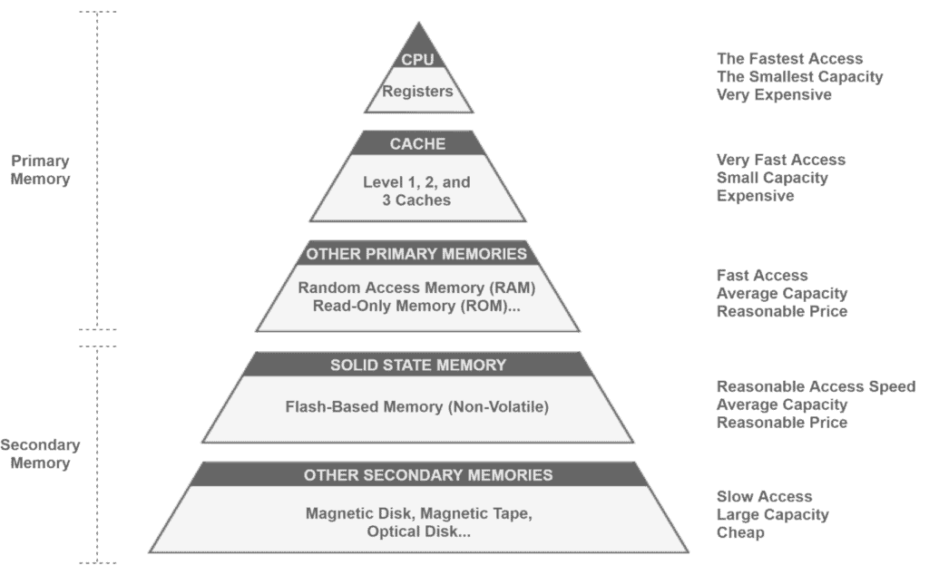
First, we should understand the concepts of primary and secondary memory to analyze each level of the memory hierarchy pyramid. The most relevant characteristic of primary memory is that the CPU accesses it directly. In contrast, the secondary memory must be allocated in the primary memory to be accessed by the CPU. By nature, primary memory is volatile, while secondary memory is non-volatile. However, there are exceptions, such as the primary and non-volatile Read-Only Memory (ROM).
2.1. The Memory Hierarchy Levels
At the top of the pyramid, we have the registers. Registers are included inside the CPU, thus presenting the fastest access time compared to the other memory devices in the pyramid. These registers compose the memory unit of a CPU. However, the memory unit shares the limited physical space of a CPU with both the control unit and the arithmetic-logic unit. So, these units must be carefully engineered and built with precision to reach the expected performance. Due to these reasons, registers usually represent the smallest and the most expensive portion of memory.
Below the registers, we have the cache memory. Due to the limitations of the CPU’s memory unit, caches provide high-speed memory close to the CPU (sometimes in particular locations of the CPU chip) connected to it with a dedicated data bus. Caches, in general, have more storage capacity and are slower and cheaper than registers. However, they are still faster, more expensive, and with low storage than other memory devices.
The third level of the hierarchy includes other primary memory devices. The most popular example of these devices is the Random Access Memory (RAM), a volatile memory that provides on-demand data to the CPU. The Read-Only Memory (ROM), Programmable Read-Only Memory (PROM), and Erasable Programmable Read-Only Memory (EPROM) are other examples of memory devices in this level.
In the fourth level, we have solid-state secondary memory, which can comprehend non-volatile flash-based devices. A prominent memory device here is the Solid State Drive (SSD). These devices read and write data without executing mechanic processes. Thus, they usually are faster, energy-economic, and more expensive than other secondary memory devices.
Other secondary devices, in turn, composes the last level of the memory hierarchy. Common examples of these devices are hard disks, optical disks, and magnetic tapes.
3. Cache Memory
Historically, the memory is speed does not evolve as the CPU speed does. However, with the evolution of the technology, CPU engineers have been making more efforts to improve the processing speed than enhancing or increasing the number of registers in the chip. Thus, memory engineers must deal with the challenges of providing high-speed memory with sufficient storage capacity and a fair cost outside the memory unit of the CPU.
The cache is an alternative to provide a fast memory very close to the CPU, using a dedicated bus to exchange data with it. In this way, memory engineers use different techniques that combine a small high-speed memory (registers plus cache, in this scenario) and large slower memory (other primary memories) to get a general speed close to the high-speed memory with a storage capacity of the slower memory.
Next, we’ll see relevant concepts and technical details regarding cache memory.
3.1. The Principle of Locality
Broadly, caches try predicting instructions and portions of data that the CPU will require shortly, loading them from other slower primary memory devices. This prediction is based on the principle of locality. The principle of locality regards the tendency that the CPU repetitively accesses specific memory regions over a certain period. Thus, in such a case, this principle refers to both temporal and spatial locality:
- Temporal locality: Assumption that recently loaded data in the cache memory will be reused several times in a short period. So, this data shouldn’t be removed or replaced from the cache during this period.
- Spatial locality: Assumption that there is a high probability that data with addresses close to the address of recently loaded data will be used shortly. Thus, the cache memory should load these related data as soon as possible.
3.2. Cache Hierarchy
The cache memory itself presents a particular hierarchy. For example, in the most common scenarios, a computer has three cache levels, called L1, L2, and L3:
- L1 cache: The fastest cache with the smallest storage capacity (typically from 16KB to 512KB). The L1 cache memory connects with the dedicated bus of each CPU’s core. In some processors, this cache divides into data and instructions cache.
- L2 cache: Cache with a slightly slower access speed than L1 cache. In usual scenarios, L2 caches present a storage capacity of 128KB to 24MB. This cache connects with the memory bus shared between pairs of CPU cores.
- L3 cache: Cache with the slowest access speed among the presented ones. Generally, the storage capacity of this cache varies from 2MB to 32MB, and it connects to memory buses shared with multiple CPU cores.
Besides the presented cache levels, particular processors, such as Haswell and Broadwell, have L4 cache memories. In such a case, L4 caches connect to memory buses shared between the CPU and GPU.
3.3. Cache Miss and Cache Hit
The CPU’s cores access the memory several times while processing a determined task. These accesses recover both instructions and data required by the CPU. It is essential to highlight that the CPU generally accesses the computer memory following the previously presented hierarchy, from faster to slower memory. For example, if the required data locates in the L3 cache, the CPU first unsuccessfully accesses the L1 and L2 caches to, finally, find the data in the L3 cache. Thus, in this small example, we can say that occurred two cache misses (L1 and L2 caches) and a cache hit (L3 cache):
- Cache miss: Event in which a cache is looked up to search for specific data or instructions, but they are not available in the accessed cache memory.
- Cache hit: Event where a cache is looked up to search for specific data or instructions, and they are available in the accessed cache memory. In this scenario, the cache returns the requested resources.
In general terms, we can say that the more hits in contrast to misses, the better is the performance of cache memory. Mathematically, we calculate the cache miss/hit ratio as follows:

Where  and
and  are, respectively, the number of cache hits and cache misses in a certain period. The
  , in turn, ranges between 0 and 1, and the closer to 1, the better is the cache performance.
Note that equal caches (in terms of hardware) processing identical data/information requests may have different performances. This difference occurs, for example, due to the adoption of distinct cache writing policies.
3.4. Context Switching
In a multitasking computer, multiple processes share the CPU execution time. In general scenarios, there are much fewer cores in the CPU than processes executing in a computer. So, the CPU schedules the execution of these processes in an interval manner. Hence, in practical terms, context switching consists of interrupting a process executing in a CPU core to execute a new process or a previously interrupted one.
While executing in a CPU core, a process will probably require multiple data and instructions, which we call the process working set. Eventually, the cache memory will load either the whole or parts of the process’ working set. However, after a context switching, the cache often is clean or contains the working set of the previously executed process. Thus, due to the context switching, several caches misses typically occur at the beginning of process execution in a CPU core.
At last, it is important to notice that the cache misses due to context switching may be more or less severe according to the storage capacity of the employed cache memory, its writing policy, and the memory workload imposed by the processes.
4. Conclusion
In this article, we studied cache memories. First, we reviewed basic concepts of computer memory. Next, we in-depth analyzed the cache memory. Then, we learned how cache memories work and the different categories of them. Finally, we outlined how the context switching in CPU cores affects the cache hits and misses.
We can conclude that caches are crucial memory devices for current computers. By using different techniques and a hierarchical structure, caches allow fast and efficient access to the computer memory, reducing CPU idleness with processes waiting for data or instructions.