

Yes, we're now running our only Summer Sale. All Courses are 30% off until 20th July, 2026:
Learn through the super-clean Baeldung Pro experience:
>> Membership and Baeldung Pro.
No ads, dark-mode and 6 months free of IntelliJ Idea Ultimate to start with.
1. Introduction
NAND and NOR flash memory are two crucial advancements in the realm of semiconductor storage, firmly rooted in Complementary Metal-Oxide-Semiconductor (CMOS) technology and perpetually propelled by Moore’s Law. These types of flash memory have revolutionized the landscape of data storage and retrieval.
Based on CMOS technology, NAND and NOR flash memory utilize a series of transistors to store and retrieve data electronically. These transistors act as switches, employing the principles of logic gates to store and retrieve information efficiently.
Moore’s Law, formulated by Gordon Moore, predicts that the number of transistors on a semiconductor chip will double approximately every two years while the cost per transistor decreases. This phenomenon has played a pivotal role in the exponential growth of NAND and NOR flash memory, enabling higher storage capacities and improved performance over time.
2. CMOS Circuits
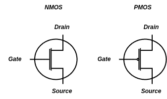
In CMOS technology, an individual transistor is built up of three components the gate, the source, and the drain. Depending on the design, an electric field is created when voltage is applied to the gate, enabling or blocking the flow of electrons between the source and drain.
For NMOS transistors, the applied gate voltage activates the transistor, allowing the flow of electrons from the source to the drain.
For PMOS transistors, the applied gate voltage switches the transistor off, preventing the flow of electrons:
CMOS technology, including NOR and NAND flash memory, is widely applied in digital circuit design. CMOS circuits utilize a combination of NMOS and PMOS transistors to perform logic functions and are characterized by low power consumption, high throughput, and excellent noise tolerance.
3. NOR Memory
NOR flash memory is called after the NOR logic gate, which is actually used in its circuitry. It was first developed in the 1980s and has been adopted widely in embedded systems such as microcontrollers, electronics, and network routers. NOR is a non-volatile storage technology meaning that it doesn’t require power to retain data.
NOR flash memory is characterized by fast random access times, which typically allow it to read relatively small amounts of data from any address quickly. It is also capable of directly executing source code from memory, which makes it appropriate for use in bootloaders and firmware.
3.1. Architecture
For the NOR gate construction, two components are connected in series, each of which consists of two transistors.
The first component comprises two NMOS transistors connected in series and the voltage supply. In comparison, the second component consists of two PMOS transistors connected in parallel along with the ground. The input is passed to the gate from each transistor, and the output is taken from the drain.
Once the input is low (0), the PMOS transistor is activated, and the NMOS is deactivated, allowing the output to be high.
In the event of a high input (1), the PMOS transistor is turned off, and the NMOS transistor is turned on, allowing the output to be low (0):
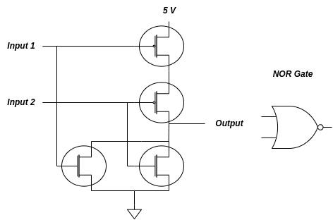
Whenever at least one of the inputs is set high, the respective NMOS transistor will be switched off, while the PMOS transistor will be switched on. As a result, the output voltage will be low.
On the contrary, if both inputs are low, then both PMOS transistors at the top will be turned off circuits, and the NMOS transistors will be open. Therefore, the output voltage is high.
4. NAND Memory
4.1. Architecture
For the NAND gate construction, two components are connected in series, each consisting of two transistors.
The first component consists of two PMOS connected in parallel along with the voltage supply, while the second component consists of two NMOS connected in series along with the ground. The input is passed to the gate of each transistor, and the output is taken from the drain.
When the input is high (1), the PMOS transistor is activated, and the NMOS transistor is deactivated, allowing the output to be low.
When the input is low, the PMOS transistor is turned off, and the NMOS transistor is turned on, allowing the output to be high:
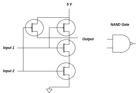
The circuit above has two inputs and one output. Whenever at least one of the inputs is low, the corresponding PMOS transistor will be conductive, while the NMOS transistor will be switched off. Accordingly, the output voltage will be high.
Instead, if both inputs are high, both PMOS transistors at the top will be open circuits, and both NMOS transistors will be conductive. Hence, the output voltage is low.
5. Performance
5.1. Access Times
NOR flash memory provides fast random access times, making it suitable for applications that require fast access to small amounts of data, such as bootloaders and firmware.
On the other hand, NAND flash memory offers slower access times because it can only be sequentially accessed, which means it requires reading or writing entire chunks of data at a given request. Hence, it is more appropriate for applications that require large amounts of storage with no respect to high access speeds.
5.2. Transfer Rates
The transfer rate depends on the amount of data to be transferred, as NAND memory has to read or write entire pages of data at a time. NOR flash memory has slower write and erases speeds than NAND flash memory, so transferring large amounts of data may take longer.
On the other hand, NAND flash memory has faster write and erase speeds, which means it can transfer large amounts of data faster.
5.3. Endurance
Flash memory has a shortened lifespan because writing and erasing data causes wear and tear on the memory cells. NOR flash memory typically has a longer endurance than NAND flash memory because it uses individual memory cells to store data, whereas NAND flash memory shares memory cells between multiple pages.
This means that each memory cell in NAND flash memory is subject to more wear than in NOR flash memory. However, technological advances have made NAND flash memory more durable than in the past, and both types of flash memory can now withstand thousands of write and erase cycles before failing.
5.4. Reliability
Flash memory can be vulnerable to data corruption and other errors, affecting the reliability of the data stored in the memory.
NOR flash memory is generally considered more reliable than NAND flash memory because it utilizes individual memory cells to store data, which decreases the risk of errors affecting multiple pages.
Yet, NAND flash memory has grown more reliable over time due to advances in error correction techniques and other technologies.
6. Applications
Mobile devices often use a combination of NOR and NAND flash memory to balance the need for fast access to small data with storing large amounts of high-density data.
Due to its architecture, NOR flash memory is used in bootloaders, firmware, and other low-density memory applications. Moreover, NOR is more suitable for fast reading of small amounts of data, which makes it preferable in microcontrollers, which are used in many embedded systems, such as appliances, automobiles, and medical devices.
On the other hand, NAND flash memory is used in applications that require high-density storage of large amounts of data. This includes solid-state drives (SSDs), USB flash drives, and other mass storage devices.
7. Conclusion
Looking ahead, both technologies are poised for exciting future extensions. Innovations in NOR and NAND flash memory will likely focus on enhancing their performance and capabilities to meet the evolving demands of connected devices and edge computing.
Ultimately, the future of flash memory will involve a balance between maximizing storage capacities and addressing the specific requirements of diverse applications, paving the way for a new era of data storage and processing.