Yes, we're now running our only Summer Sale. All Courses are 30% off until 20th July, 2026:
Guide to the CPU
Last updated: March 20, 2023

Learn through the super-clean Baeldung Pro experience:
>> Membership and Baeldung Pro.
No ads, dark-mode and 6 months free of IntelliJ Idea Ultimate to start with.
1. Introduction
In this tutorial, we’ll look at how the central processing unit (CPU) works collaboratively with the other important components such as the arithmetic logic unit (ALU), registers, and RAM.
2. Overview of the CPU
There are so many jobs that the CPU is responsible for. It is simply the heart of any computer. Programs such as Firefox, Sublime Text, or GTA V, are made up of a sequence of operations known as instructions. They tell the computer what to perform. If the instructions are mathematical such as add or subtract, the CPU will set its ALU to perform this mathematical computation. It could be a memory instruction as well. In that case, the CPU will interact with the memory to read and write values.
In order to perform these kinds of complicated operations, there are a lot of parts in the CPU as we can see in the figure below. We’re going to focus on some blocks rather than examining every single wire. This level of view such as in the figure below is called microarchitecture:
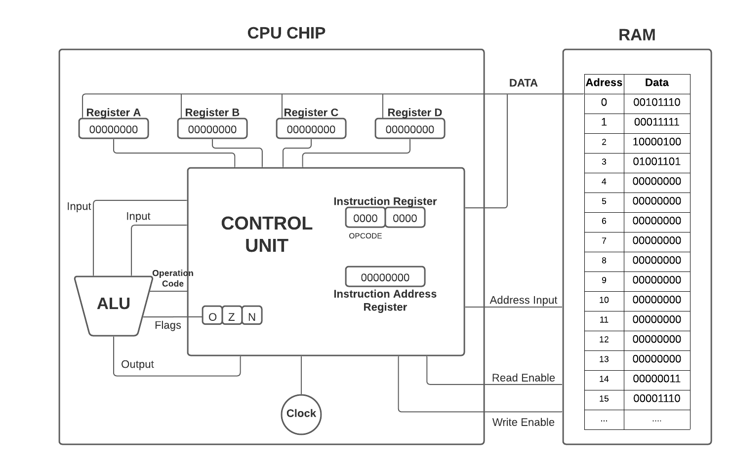
We need to have some memory to run a program. In order to keep things simple, we’ll use a memory that has 16 memory locations, each contains 8 bits. Furthermore, as we can see in the figure, our processor has four 8-bit memory registers, A, B, C, and D. We’ll use them temporarily to store and manipulate values.
2.1. Instruction Tables
Data can be stored in memory as binary values and as we’ve said programs can be stored in memory too. CPUs have some instructions table to specify supported instruction by assigning an ID to them as we can see in the table below. In our example, the first four bits will be our operation code or opcode for short. The other four will be the data for that operation. The data may come from registers or an address in memory.
CPU also needs two more registers which are the instruction address register and instruction register. In order to keep track of where we are in a program, we use an instruction address register. It stores the memory address of the current instruction. When we first boot up our computer, all of these registers start at 0. We initialize our RAM with a tiny program that we go through in this article.
We can see the instruction tables below:
| Instruction | Description | 4-Bit Opcode | Address or Registers |
|---|---|---|---|
| LOAD_A | Read RAM location into register A | 0010 | 4-bit RAM address |
| LOAD_B | Read RAM location into register B | 0001 | 4-bit RAM address |
| STORE_A | Write from register A into RAM location | 0100 | 4-bit RAM address |
| ADD | Add two registers, store result into second register | 1000 | 2-bit register ID 2-bit register ID |
2.2. Instruction Cycle
In order to process instructions, the CPU should follow the instruction cycle, which simply includes fetch, decode and execute cycles, from boot-up until the computer has shut down. The first phase of a CPU’s operation is called fetch phase where we retrieve our first instruction.
Since the register value is 0, the RAM returns whatever value is stored in address 0. In this case, 00101110. Then this value is copied into the instruction register. So, now that we’ve fetched the instruction from the memory. We’ll need to figure out what this instruction is so the CPU can execute it properly. This is called the decode phase.
In the decode phase, the opcode is the first 4 bits: 0010. This corresponds to the  instruction which loads a value from RAM into register A. The RAM address is the last four bits: 1110, or 14 in decimal.
These operations are performed through logic gates. Without going into details so much we can say that the control unit is responsible for directing all the different parts of the CPU. After having completed one full fetch, decode, and execute cycle, we’re ready to start all over again. If we carefully look at the first 4 rows of the memory and the instruction table, we can see that in the cycle, we have  as the opcode 0001, and the RAM address:1111. We save the value 00001110, 14 in decimal into register B.
2.3. Add Instruction
If we increment the instruction address register one more time it’ll address the 2. In address two we have 1000 as the opcode. It turns out that our next instruction is  instruction which adds the values in two registers and stores result in the second register. The CPU carries out this operation with the help of the ALU. If we look at the final 4-bits of the instruction, we can see 01 corresponds to register B and 00 corresponds to register A. At the end of this instruction, our CPU adds 14 and 3, and stores 17 into register A.
2.4. Store Instruction
Now, we can fetch the last instruction: 01001100. If we decode it we can see that 0100 is a  instruction, with a RAM address 1100, which is 12 in decimal. We pass the address to the RAM, rather than read-enabling the memory, we write-enable it.
To sum up, we loaded two values from memory, added them together, and then saved the result into memory.
3. CPU Clock
CPU clock is responsible for keeping the CPU ticking along fetch, decode, and execute phases. It triggers an electrical signal at regular intervals. The control unit uses it to advance the internal operations of the CPU.
The speed at which a CPU can perform each step of the fetch, decode, execute cycle is called its clock speed. This speed is measured in Hertz, a unit of frequency. One hertz means that one cycle per second.
One of the first CPUs, the single-chip CPU the Intel 4004, is a 4-bit CPU and is released in 1971. Its microarchitecture is quite similar to our example of CPU. While its clock speed is 740 Kilohertz, which means 740 thousand cycles per second, today’s modern computer processors’ clock speed is a few gigahertz that means billions of CPU cycles every single second.
4. Conclusion
In this article, we’ve discussed how the CPU works and demonstrated a simple program that runs on the CPU. We’ve given details about the instruction tables, instruction cycle, and the CPU clock as well.